Layout Guidelines for High Frequency PCB
Layout Guidelines for High Frequency PCB
High frequency pcb are used in advanced communication systems like GPS, radar, and base stations. These PCBs require strict layout guidelines and termination schemes to avoid issues like ringing, ground bounce, reflections, and impedance mismatches.
A good quality PCB requires proper planning and selection of the right materials. This will prevent any setbacks during the manufacturing process.
Choosing the best circuit material
Choosing the best circuit material is an important step in the fabrication of high-frequency PCBs. The choice of the substrate material can have a significant effect on signal loss and impedance control. There are many different materials to choose from, and each one has its advantages and disadvantages. The substrate is a non-conductive material that acts as the foundation for the conductive parts of the PCB. It is usually chosen based on its dielectric constant, or DK. The substrate also provides insulation between the conductive layers, and it may have more than one layer for multilayer boards.
The substrate material must be able to handle the voltages and currents that are required for the high-frequency signals. It must also be able to resist the effects of temperature, vibration, and moisture. In addition, the selected substrate material must have a low dissipation factor and low water absorption rate. It is essential that the PCB’s insulation and moisture are in good condition, as these factors can affect signal integrity.
In determining the best circuit material for high-frequency pcbs, it is necessary to consider several factors, including the size of the interconnects and their location. It is also important to know how much copper is required for each pair of interconnects. It is essential to avoid using materials that require a large amount of copper, as these can cause excessive signal losses.
Designing
Creating a high-frequency PCB requires attention to detail in almost all aspects of the layout. This includes component placement, spacing and clearances, routing, stackup, grounding, and materials selection. Choosing the best materials will ensure that your board is capable of handling the high frequencies required for signal transmission and keeping your components functioning in top condition.
High-frequency circuits require a lower imaginary part of the dielectric constant (Dk). This is because longer wires cause more losses and can affect the impedance. In addition, a lower Dk will help you avoid problems such as common mode noise and interference.
Another important consideration is to use a high-speed laminate for the outer layers of your PCB. This will provide better high frequency pcb conductivity and shielding. It will also help prevent RF interference and maintain the integrity of your circuits.
To avoid interference between adjacent signal lines, you should apply the 20H rule. This rule states that the signal plane should be much thinner than the power plane. This will prevent the coupling of electromagnetic waves between signal lines, which is called crosstalk. Moreover, you should try to avoid using vias in your design. They can High Frequency PCB Supplier introduce 0.5 pF distributed capacitance that can interfere with the signal transmission process and lead to data error. Moreover, you should not use loops in your PCB, as they can lead to signal degradation and increase the power loss.
Fabrication
Creating the best high-frequency PCB requires careful planning. It is important to know the frequency of the signals, the power and voltage demands, whether they need to be divided, and what kind of space will be required. This will help in determining the appropriate layer stackup. In addition, it is also essential to have a solid understanding of what materials are appropriate and how they will work together. This will ensure the highest signal integrity.
High-speed PCBs require higher density interconnects, which can cause a large amount of heat to build up in the board. This is why focusing on the PCB material is so important. The material must have a low dielectric constant, CTE, and loss tangent. It must also have good mechanical stability. In addition, it should be able to handle temperature variations.
The fabrication process for high-frequency PCBs includes printing copper for the inner layers. The outer and inner layers are then laminated together. This step is crucial for high-frequency PCBs because it allows the copper to be pre-bonded on the exact laminate that serves as the circuit board structure. After that, the copper is engraved to unveil the initial PCB blueprint. A high-frequency PCB also needs to have a high-density layout of heat dissipation holes. However, this is not easy to achieve. The drilling process can create melted debris that solidifies on the hole walls, which compromises the quality of the holes. This can also affect the signal quality.
Testing
In high-frequency PCBs, the quality of signal integrity is very important. Ideally, the signal should travel from a source to a sink without any interference or degradation. However, this does not always happen in practice due to signal loss (impedance mismatch, crosstalk, attenuation, reflection, and switching issues). Signal integrity analysis is an essential part of the design process. It can detect and prevent problems that may not be obvious in a prototype. It can also help determine the best board material for the design.
When selecting a high-frequency PCB, look for one that has a low dissipation factor and a stable dielectric constant. This will help ensure that the rate of signal transmission is not affected by the laminate thickness. It is also advisable to use a material with a low coefficient of thermal expansion, which will minimize separation between the copper foil and the laminate.
Another thing to consider is the size of the through hole. Larger holes can cause the insertion loss of the circuit to increase, which is not ideal for high-frequency applications. You can avoid this problem by using a through-hole insulator.
In addition, you should consider routing the frequency signals carefully. This will help you prevent interference between different signals and reduce radiated EMI. The best way to do this is by following the 20H rule, which states that the ground plane should be much thicker than the power plane.
You May Also Like
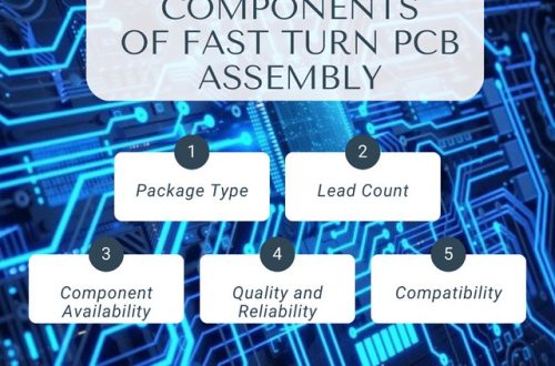
Title: The Complete Guide to PCB Assembly
The Benefits of Privacy Window Film